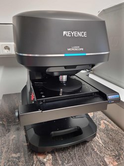
3D Confocal Laser Scanning Microscope
The microscope is used for the characterisation of surface by recording and analysing 3 dimensional surface topographies. The laser beam scans the surface in x and y direction while a stepwise change of the focus point is achieved via the objective. The microscope is applied to analyse surface subjected to mechanical loading, e.g. after tribological tests, to measure 3 dimensional structure in microelectronics and nanoelectronics, to measure the thickness of opaque and transparent films as well as to determine the surface roughness.
Technical data:
- Device: Keyence VK-X1100
- Laser Wavelength: 404 nm
- Objectives: 5x, 10x, 20x, 50x and 150x
- Sample Stage: 100 mm x 100 mm
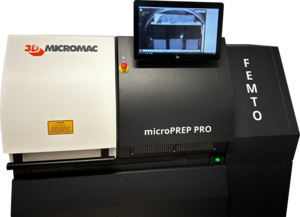
Laser ablation system microPREP™ PRO FEMTO
Our laser ablation system, the microPREP™ PRO FEMTO, offers a groundbreaking solution for precise material processing and sample preparation. Equipped with a state-of-the-art femtosecond laser, it enables material removal with micrometer precision while minimizing thermal effects on the material. This system facilitates the rapid and straightforward production of sample structures, such as microtip arrays [1] and half-grids [2], directly from the material, paving the way for revolutionary advancements in correlative microscopy [3].
Microtip arrays are coupons with 15 tips (radius <30 µm) that can be finalized for atom probe tomography (APT) in just a few steps using focused ion beam (FIB) technology. By eliminating the need for complex lift-out procedures, the system reduces effort and enhances the reliability of sample preparation. Half-grids, on the other hand, are semicircular structures that enable the simultaneous application of APT and transmission electron microscopy (TEM) on the exact same site, significantly simplifying correlative microscopy.
The combination of femtosecond laser technology and electron backscatter diffraction (EBSD) allows for the precise preparation of site-specific features, such as grain boundaries. These capabilities make the microPREP™ PRO FEMTO an indispensable tool for cutting-edge materials research [3].
Highlights
- High-precision processing enabled by femtosecond laser technology
- Versatile for various sample structures and material types
- Optimized for advanced research needs, meeting the highest scientific standards
Technical Data:
- Wavelength: 515 nm
- Pulse duration: 230 fs
- Maximum power: 2.5 W
- Repetition rate: 60–1000 kHz
- Laser spot diameter: <10 µm
- Sample holders: X-Y stage and rotational sample holder
[1] M. Tkadletz, H. Waldl, M. Schiester, A. Lechner, G. Schusser, M. Krause, N. Schalk, Efficient preparation of microtip arrays for atom probe tomography using fs-laser processing, Ultramicroscopy 246 (2023). doi.org/10.1016/j.ultramic.2022.113672.
[2] M. Tkadletz, M. Schiester, H. Waldl, G. Schusser, M. Krause, N. Schalk, fs-laser preparation of half grid specimens for atom probe tomography and transmission electron microscopy, Mater Today Commun 39 (2024). doi.org/10.1016/j.mtcomm.2024.108672.
[3] J. Tang, O. Renk, M. Tkadletz, Site-specific femtosecond laser ablation: The pathway to high-throughput atom probe tomography characterization, Mater Charact (2024) 114618. doi.org/10.1016/j.matchar.2024.114618.
Raman Spectroscopy
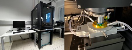
Raman spectroscopy can be applied for the characterization of chemical bonds, phase changes or oxidation processes of construction and functional materials. The underlying Raman effect is based on the inelastic scattering of the light from a laser on the molecules within a sample. Thus, the chemical fingerprint of the sample can be characterized both laterally and depth resolved. Raman spectroscopy can be applied for a variety of material classes, for instance ceramics, polymers and semiconductors. Using the attached heating chamber allows to investigate the material behavior in-situ up to a temperature of 1500 °
Technical data:
- Device: Witec alpha300 R
- Wavelength of laser: 532 nm
- Lateral resolution: 250 nm
- Depth resolution: 1 µm
- Temperature regime: between room temperature and 1500 °C
X-ray Diffractometer
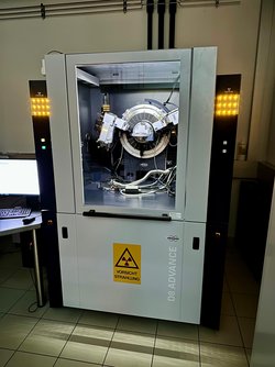
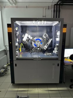
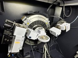
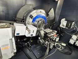
To analyze the crystallographic structure of thin films, powders, and crystalline bulk materials, two high-resolution X-ray diffraction (XRD) systems from Bruker’s D8 series are available: a D8 DISCOVER for complex thin film systems and a D8 ADVANCE for precise powder analyses. These instruments enable phase identification and quantification, texture and residual stress measurements, as well as in-situ investigations under variable atmospheric conditions.
Using monochromatic Cu-Kα radiation and energy-resolving detectors, reflections at the crystal lattice can be detected and analyzed with high precision. Advanced components such as the EIGER2 R 500K detector with 0D, 1D, and 2D capabilities and modular optical systems ensure top data quality alongside flexible configuration options. The use of a Eulerian cradle and precision motorized axes further allows detailed investigation of textures and residual stresses in samples of various geometries. The versatile equipment setup, including interchangeable optics, adaptable sample holders, and specialized chambers, also enables complex measurement routines – from grazing incidence and reciprocal space mapping to high-temperature and reactive environment studies under controlled atmospheres.
Technical data:
- • Measurement geometries: Bragg-Brentano, parallel beam, grazing incidence, transmission, reflection
- • Radiation: Copper K-alpha, line and point focus
- • Detectors: LYNXEYE XE-T (0D/1D mode) and EIGER2 R 500K (0D/1D/2D mode)
- • Sample holders: Multi-sample holder, Eulerian cradle, capillary holder, high-temperature chamber (up to 1200 °C), and reaction chamber
- • Atmospheres: Vacuum, air, and reactive gases
- • Software: ICDD PDF database 2023 and EVA (phase analysis), TOPAS (quantitative phase determination, Rietveld refinement), TEXTURE (texture analysis), LEPTOS (stress calculation)
How to XRD:
Watch the video: XRD_Advance_Video.mp4

