Quenching- and Deformation Dilatometer
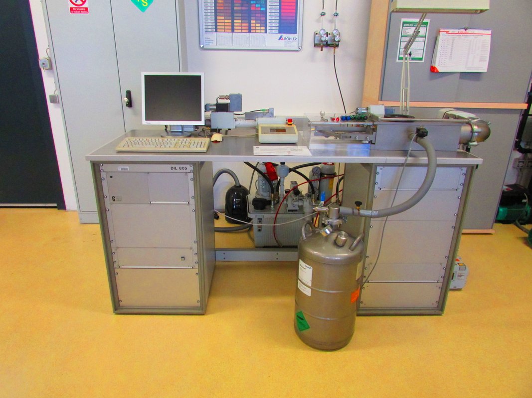
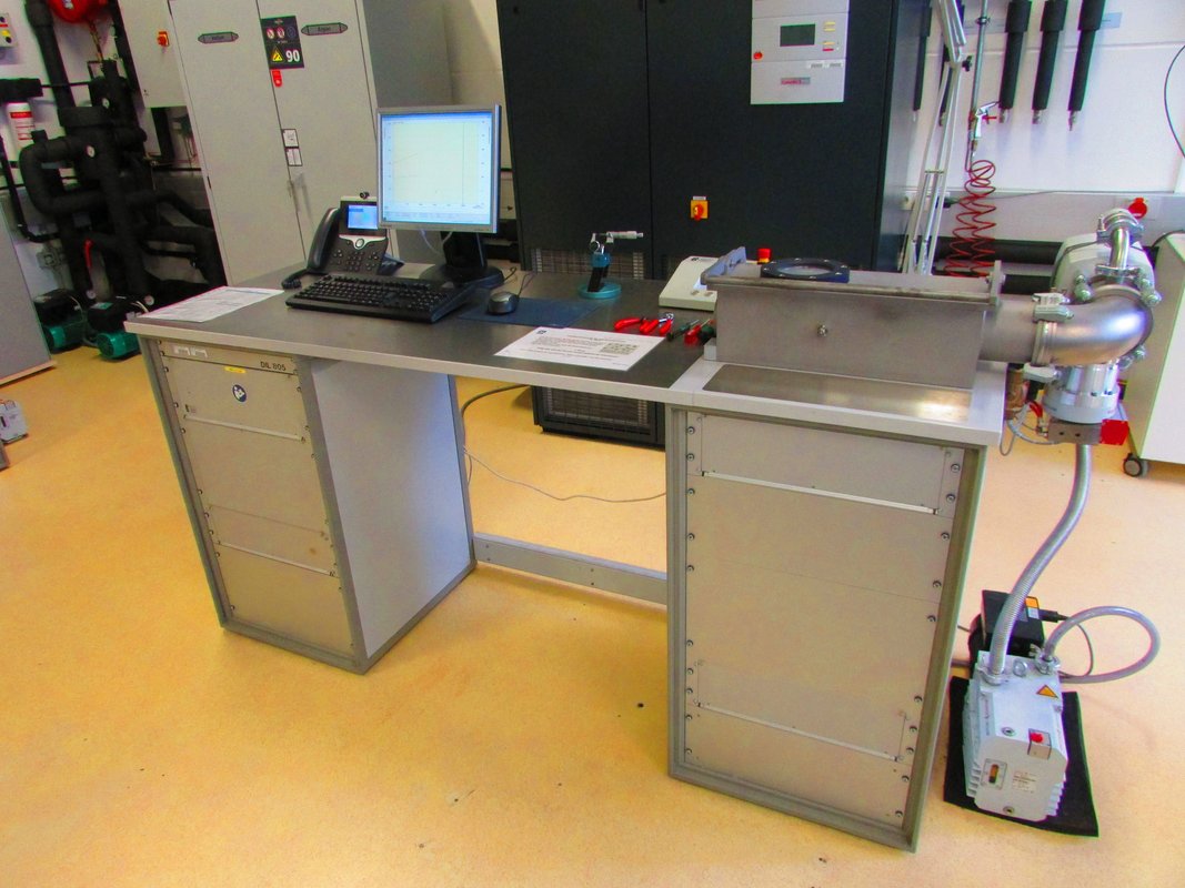
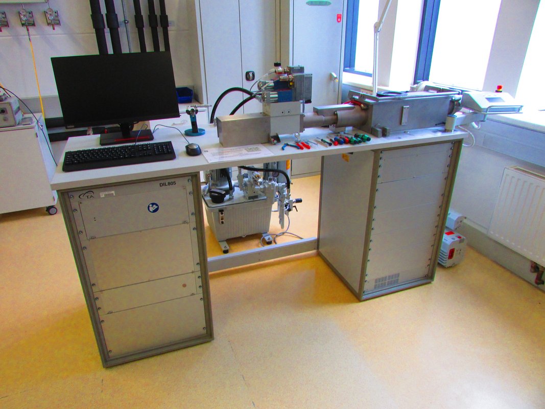
A so-called quench dilatometer is suitable for the determination of phase transformations under industrial relevant heating and cooling conditions. Three devices (TA Instruments DIL805 A/D/T and DIL805 A) are available at the department. The former is equipped with a tensile/compression deformation unit, which is used to determine the deformation behaviour of the tested material. The specimen is inductively heated by a water-cooled double-walled coil and cooled through the inlet of gas into the chamber. The change in length is recorded as a function of time or temperature or the degree of deformation. From this, for example, continuous and isothermal time-temperature transformation diagrams (TTT) as well as deformation-time-temperature transformation diagrams (DTTT) can be generated.
Main applications: Determination of thermal expansion coefficients, kinetics of phase transformations, generation of TTT, TTA and DTTT diagrams, generation of flow curves, simulation of heat treatments and deformation processes.
Technical data:
Quenching Dilatometer:
- Temperature range: 20°C to 1500°C, cryogenic temperatures -200°C to 1100°C
- Heating: inductive
- Atmosphere: nitrogen, helium, vacuum, air
- Heating rate: max. 4000 K/s
- Quenching rate: max. 2500 K/s
- Resolution: 50 nm, 0,05°C
- Specimen geometry: round samples, length 10 mm, diameter 3-5 mm, Cryogenic samples only with hollow round samples, diameter 4-5 mm
Deformation Dilatometer:
- Temperature range: 20°C - 1500°C
- Heating: inductive
- Atmosphere: nitrogen, helium, vacuum, air
- Heating rate: max. 100 K/s
- Quenching rate: max. 100 K/s
- Resolution: 50 nm, 0,05°C
- Specimen geometry: round samples, length 10 mm, diameter 3-5 mm, round and and flat tensile samples
- Forming speed: compression: 0,001 to 20 s-1, tension: 0,001 to 1 s-1
- Degree of deformation: 0,01 to 1,2
- Compressive force: max. 20 kN
- Tractive force: max. 10 kN
Atom probe tomography
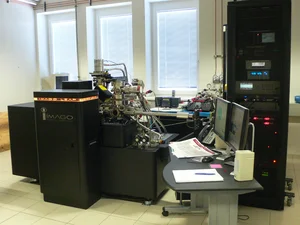
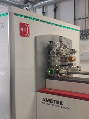
For the characterization of materials with near-atomic resolution, Atom Probe Tomography (APT) is of special interest. For such investigations, an atom probe of the type LEAP 5000 XR, as well as a LEAP 3000X HR from Cameca Inc. are available.
In atom probe tomography, a DC voltage of several kilovolts (5-15 kV) is applied to a tip with a tip radius of 20-50 nm. By means of a superimposed voltage or laser pulse, atoms are removed from the surface by the effect of field evaporation and accelerated onto a position-sensitive detector. The detector simultaneously records the time of flight as well as the positions of the arriving ions, enabling a 3D reconstruction of the ablated tip providing information about its chemical structure. Almost the entire periodic system can be resolved by the atom probe. By the use of a laser pulse, materials with poor electrical conductivity can also be analysed. Especially the UV laser (wavelength: 355 nm) of the LEAP 5000 XR enables investigations on of complex materials, ceramics and even geological materials.
Main applications: precipitation reactions, grain boundary segregation, chemical clustering, multifunctional thin films
Technical data:
LEAP 5000 XR:
- Temperature range: 20K to 100K
- Imaging gas: Neon, Helium, Argon
- Field of view: > 150 nm
- Mass resolution: FWHM > 1100
- Laser: UV (wavelength: 355 nm)
LEAP 3000x HR:
- Temperature range: 20K to 120K
- Image gas: Helium, Neon
- Field of View: < 200 nm
- Mass Resolution: FWHM ≤ 1100
- Laser: green (wavelength: 532 nm)
Differential Scanning Calorimetry (DSC) and thermogravimetric analysis
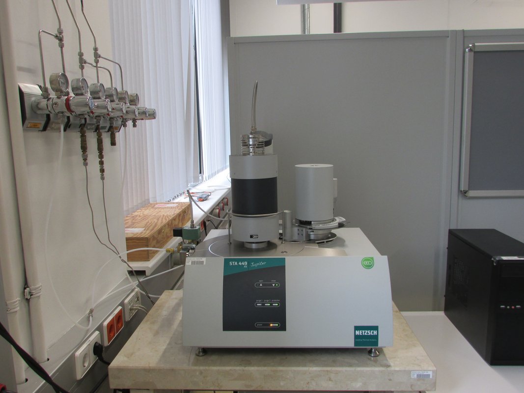
Dynamic methods are particularly suitable for efficient determination of phase transformation temperatures. A thermal analysis unit with autosampler is available at the department for this type of measurement. The unit is a combination of a dynamic differential calorimeter and a thermogravimeter. In differential scanning calorimetry (DSC), samples of known mass and suitable reference sample are subjected to a defined temperature program. Due to the thermal energy released or consumed during transformations in the sample, heat flow differences, which occur between the sample and the reference are recorded. This allows the determination of kinetics and temperature range of phase transformations, as well as reaction enthalpies. Thermogravimetry also detects changes in mass. Thus, for example, oxidation processes or decomposition reactions can be monitored.
Technical data:
Netzsch STA 449 F5 Jupiter:
- Measuring principle: dynamic differential calorimetry
- Temperature range: RT up to 1600°C
- Heating- and cooling rate: 0,001 K/min - 50 K/min
- Atmosphere argon, helium, synthetic air, vacuum (10^-2mbar)
- Resolution: 1 µW
- Resolution Scale: 0,1µg, Drift <5µg/h
- Autosampler up to 19 samples
Focused Ion Beams
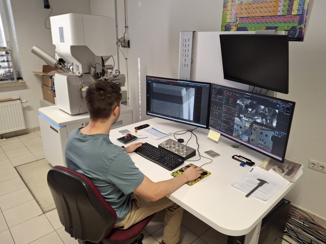
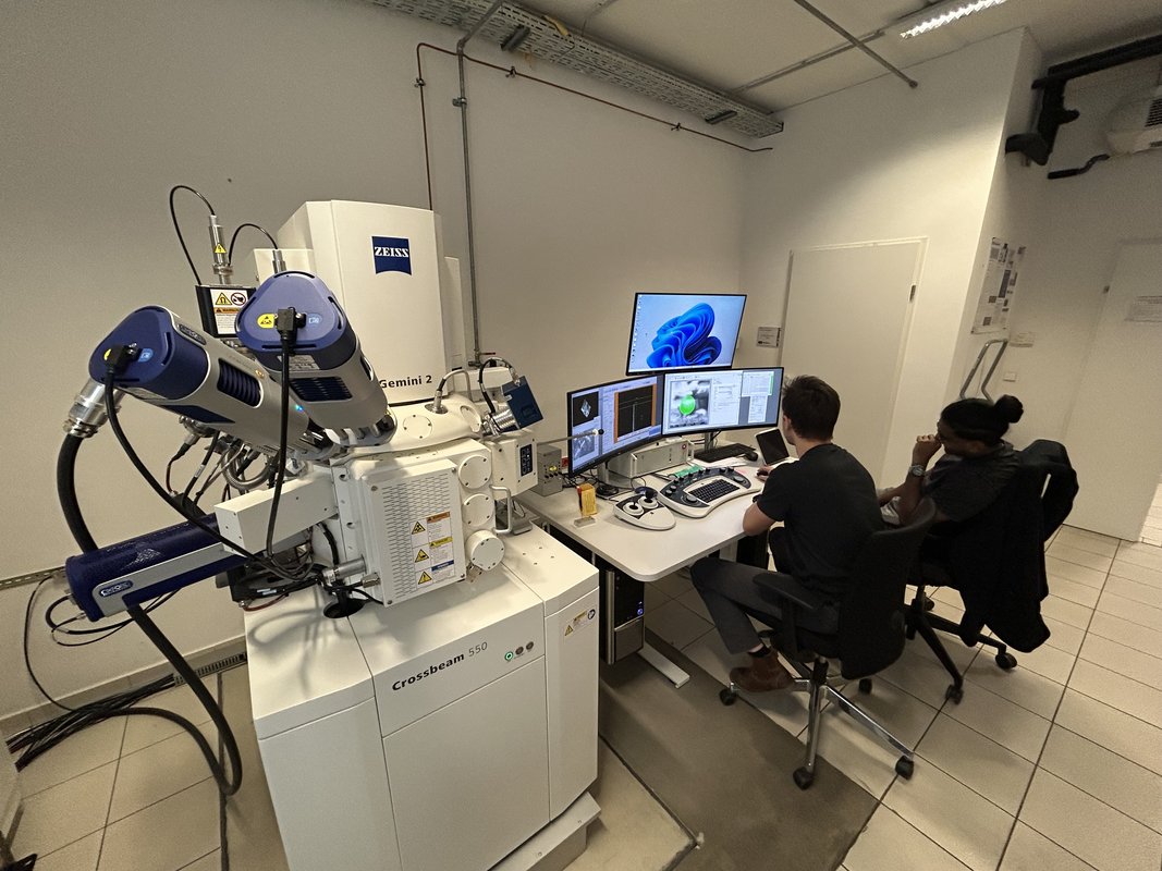
Site-specific sample preparation for transmission electron microscopy (TEM) and atom probe tomography (APT) requires specialized techniques. Two DualBeam focused ion beam (FIB) instruments are available at the department for this purpose: a Tescan Amber and a Zeiss Crossbeam 550. These microscopes feature both a focused ion beam (FIB) and an electron beam (SEM). This dual-beam capability allows for cross-sectional imaging while the sample is being mechanically milled out using the ion beam. Furthermore, both microscopes are equipped with EDX and EBSD systems from Oxford Instruments. The EDX system enables the determination of the chemical composition of the analyzed sample area, while an EBSD detector allows for the determination of crystal orientations.
Main applications are: sample preparation for SEM, TEM and APT; texture analysis.
Technical data:
- Electron beam: Field emission emitter, 1 nm resolution
- Electron beam accelerating voltage: 200 V – 30 kV
- Ion beam: High-current ion beam with Ga liquid-metal ion source
- Ion beam accelerating voltage: 0.5 – 30 kV
- Detectors: SE, SI, BSE, STEM, Axial/MD, In-lens
- Gas Injection System (GIS): Platinum
- Micromanipulator
- Plasma cleaner
High temperature laser confocal microscope
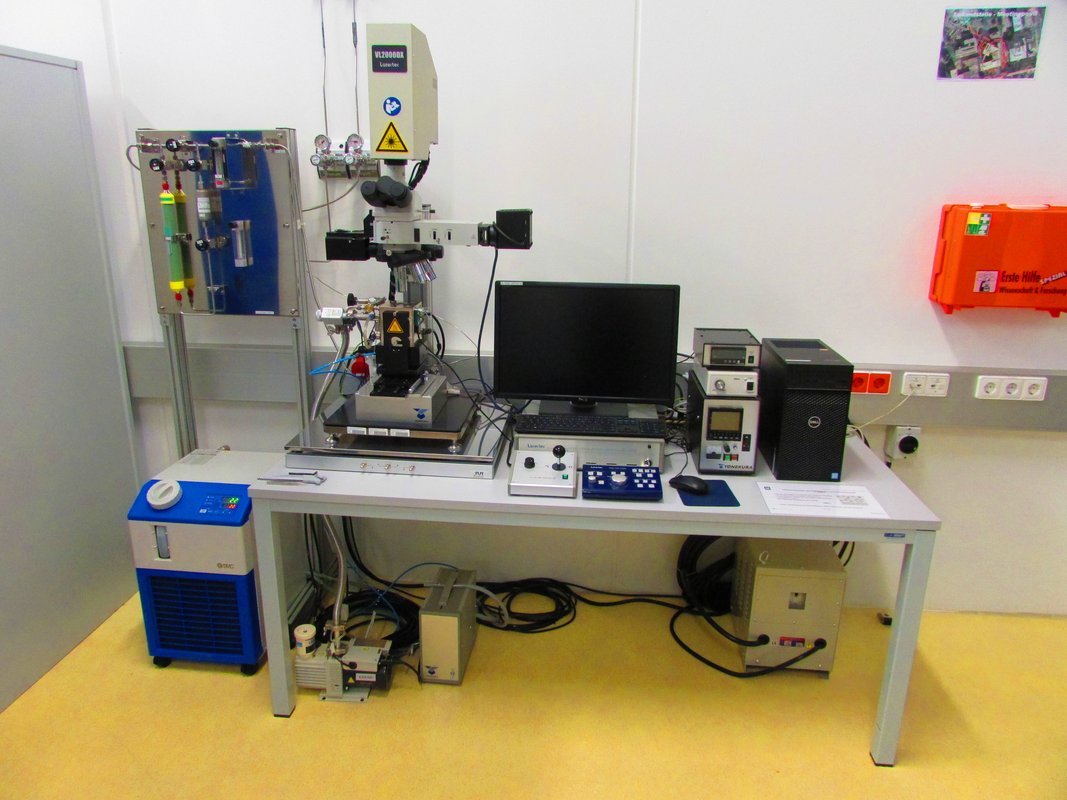
For in-situ observations of microstructural transformations, a Yonekura VL2000DX-SVF17SP high-temperature laser confocal microscope is available at the department. In the high-temperature chamber, which works according to the mirror furnace principle, the sample is heated by a halogen lamp and thus subjected to a predefined heat treatment. Any heat treatment up to a short-time temperature of 1800°C can be performed under argon atmosphere.
In this process, the microstructure becomes visible by thermal etching. A laser beam scans the sample surface, is reflected and detected by a light sensitive detector. A pre-set number of individual images, as well as a real-time video, are generated during the experiment. The device is suitable for investigating microstructural transformations during heating and cooling processes. Processes such as microstructural changes, grain coarsening or precipitation processes can be monitored in real time.
Technical data:
- Temperature range: 20°C - 1800°C (continuous temperature 1700°C)
- Heating system: mirror furnace principle with 1.5 kW halogen lamp
- Atmosphere: argon
- Heating and cooling rate: max. 6000 K/s (reasonable up to approx. 1000 K/min with helium as quenching gas)
- Maximum resolution: 0.14 µm
- Frame rate: 1 to 15 Hz
- Specimen geometry: standard cylinder specimen diameter 5mm, specimen height 1mm, polished with 3µm suspension, unetched
Ion milling systems Hitachi IM5000
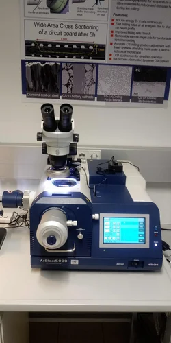
Ion milling systems are widely used as instruments for preparing surfaces as well as cross-section samples for scanning electron microscopy (SEM), with applications to fields such as materials science and semiconductor research. The two types of ion-milling methods commonly used for SEM samples are flat milling and cross-section milling1)
Cross-section Milling
Used to produce wider, undistorted cross-sections without applying mechanical stress to the sample
Flat Milling
Used for removing surface layer artifacts and final polish after traditional mechanical polishing techniques.
Technical data:
- Ar ion gun, max. 8KV accelerating voltage
- Max. milling rate >1mm/hr for Si
- Cross-section and flat milling sample holder
- Max. sample size 20mm (cross-section), 50mm (flat milling)
Scanning electron microscope (SEM) Tescan Clara
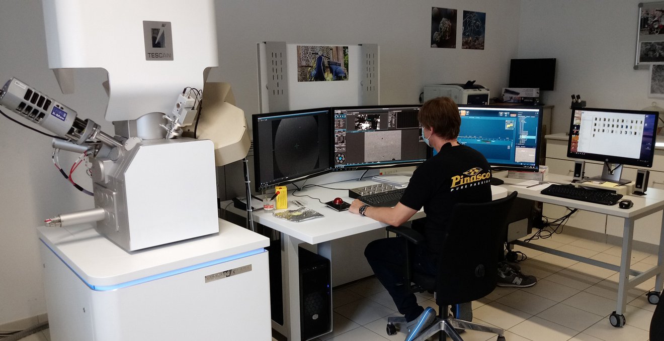
SEM is widely used to study the microstructure and the chemical composition of a wide range of organic and inorganic materials. The electron beam, focused by an electromagnetic lens system, is scanning across the sample’s surface, which is located in an evacuated specimen chamber. Due to the interaction between electron beam and sample several signals are generated, which can be measured by various detectors. These signals provide information from the topography, the chemical composition and the microstructure.
Technical data:
Field Emitter SEM
Resolution: 0.9 nm with 15 kV, 1.6 nm with 1 kV
Acceleration voltage: 200 V to 30 kV
Detector: SE, BSE, InBeamSE, InBeam BSE with energy filtering Beam Deceleration, Plasmacleaner
EDX and WDX system by Oxford Instrument
Microscopy – Failure analysis
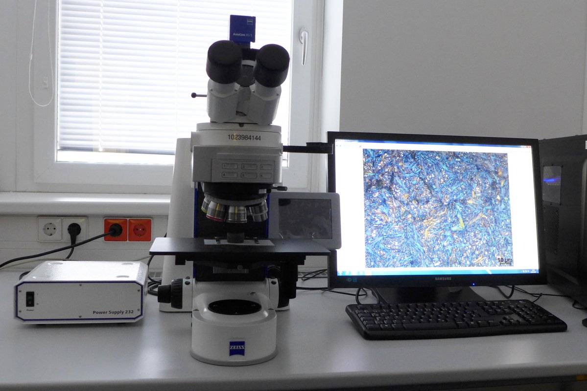
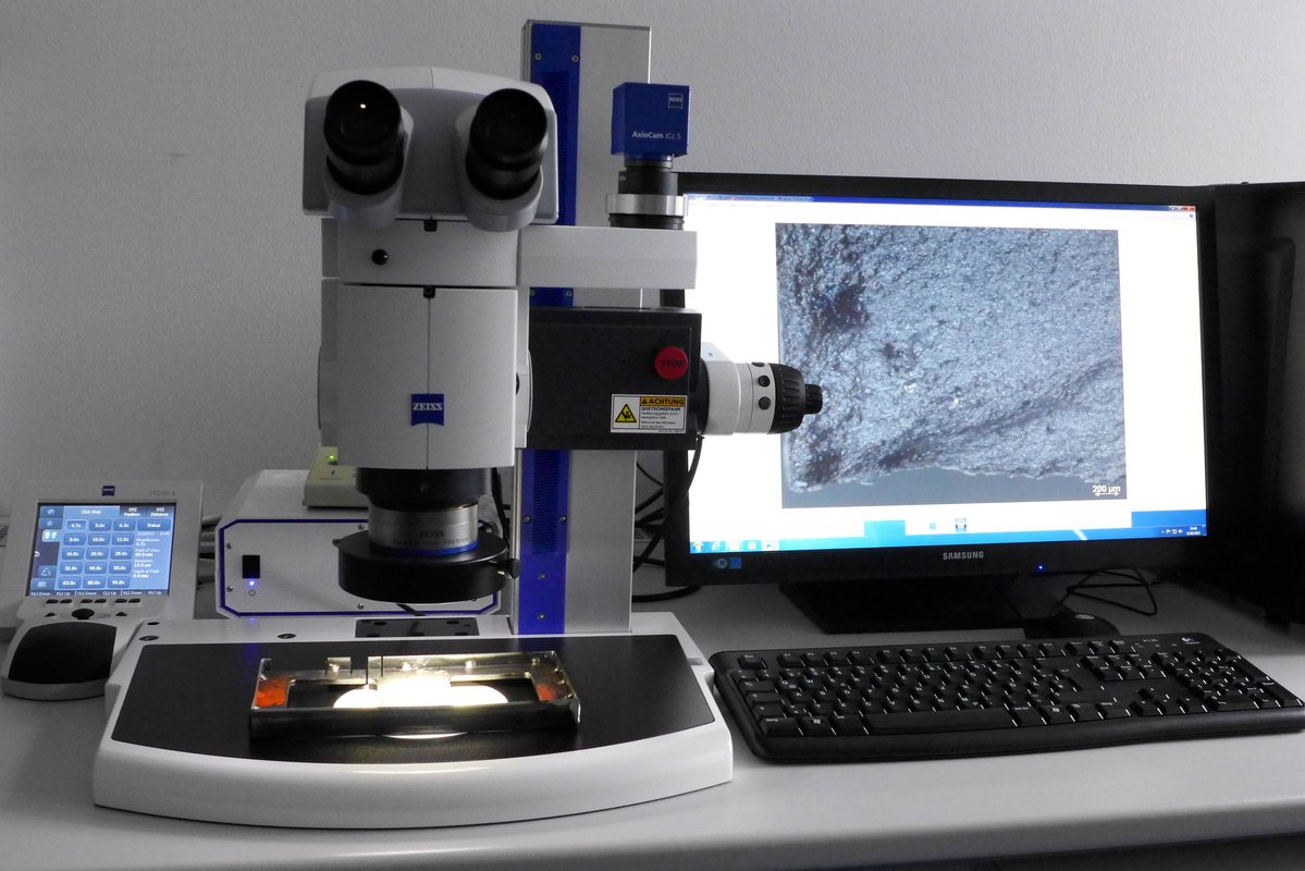
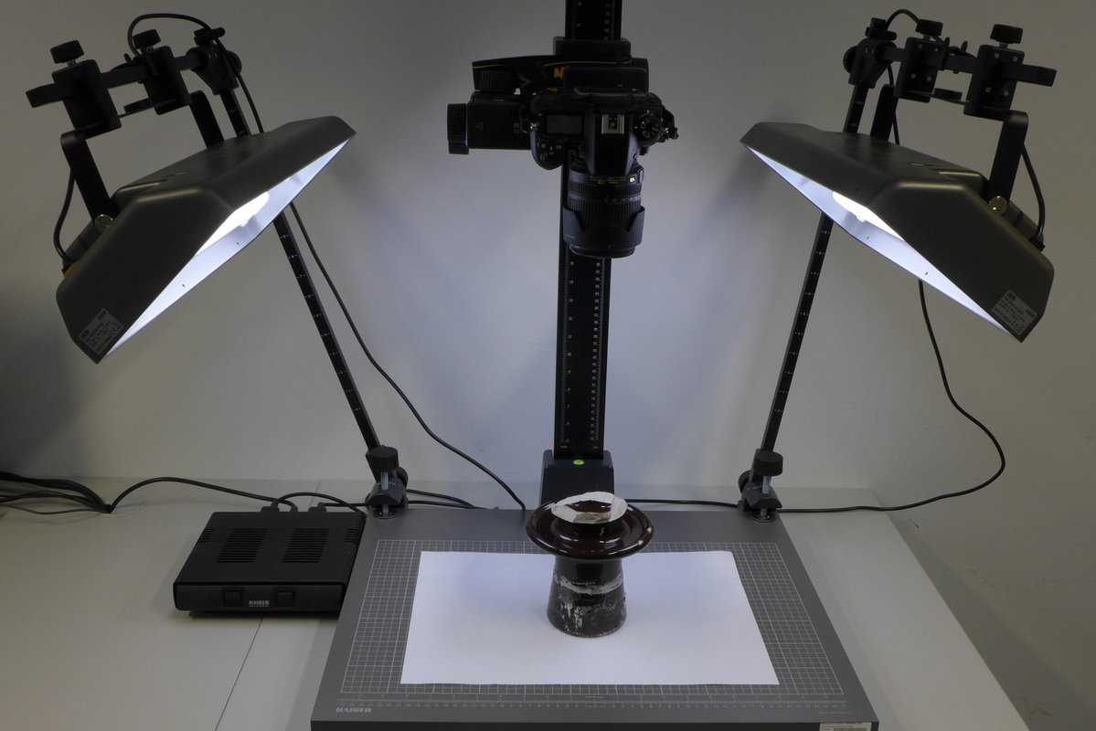
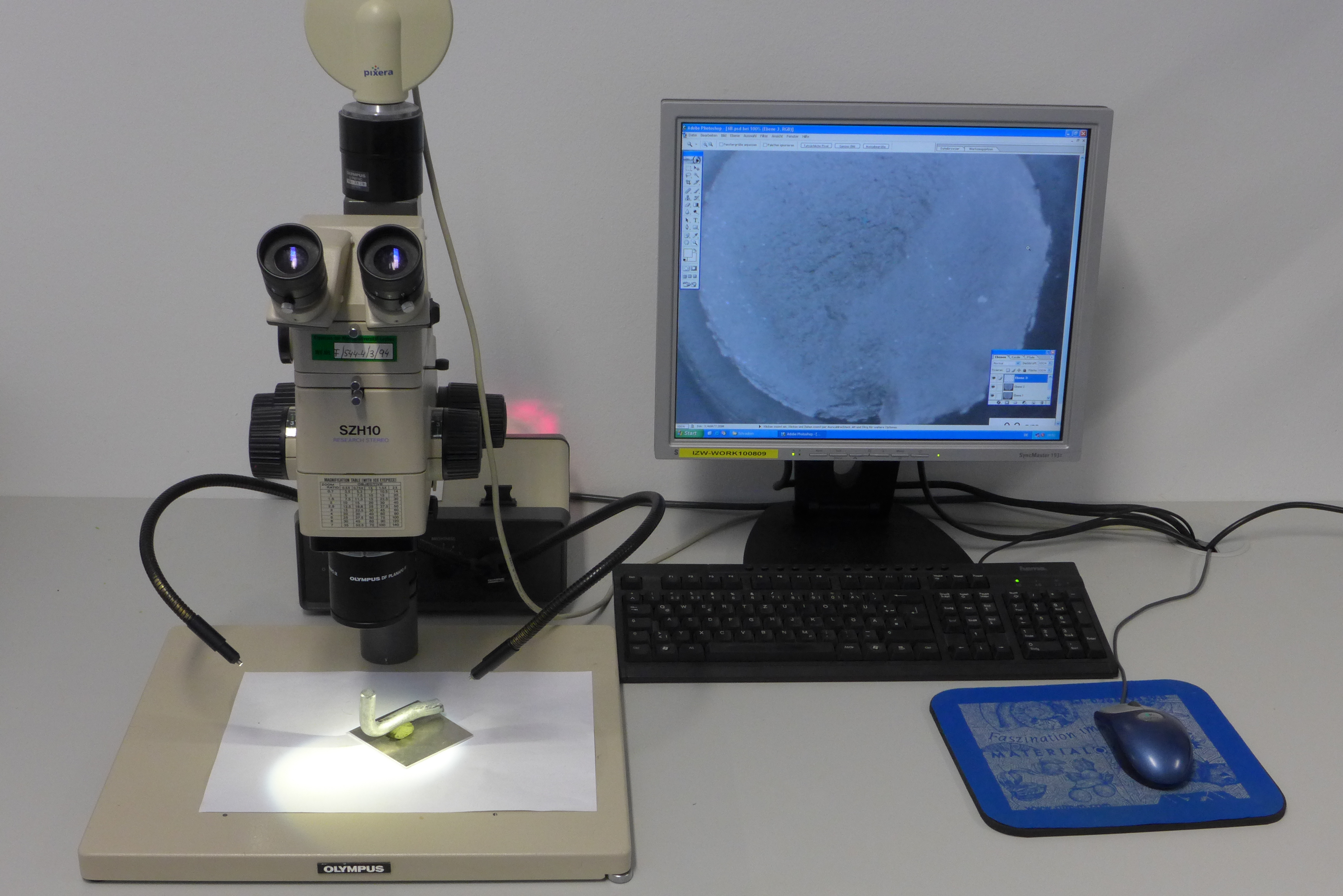
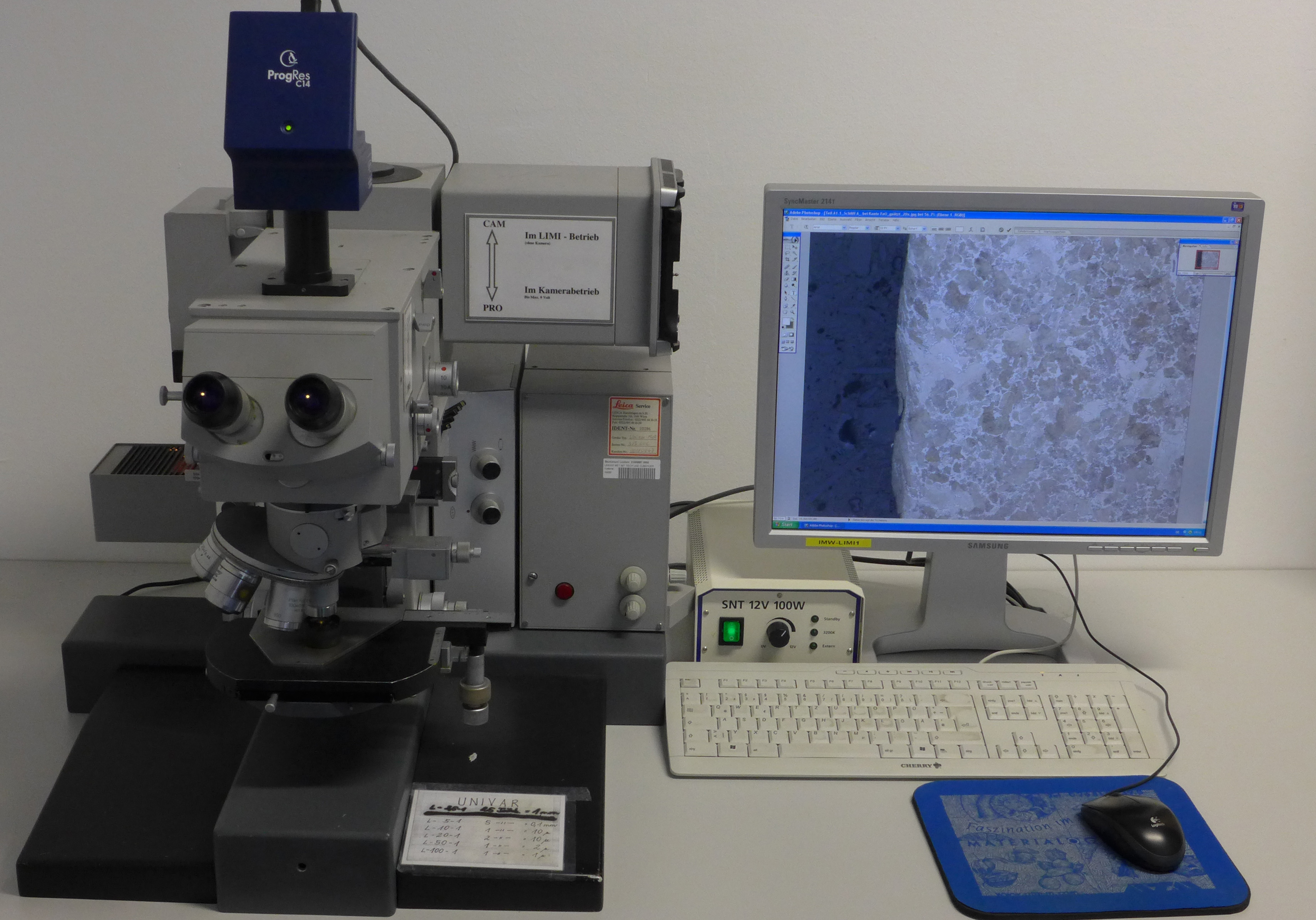
To clarify failure claims mostly photo-optical devices are used. For the macroscopic and microscopic assessment of failure claims stereomicroscopes and reflected-light microscopes, respectively, can be used by students during the tutorial failure analysis. All microscopes are equipped with a depth of focus correction.