Biaxial Stress Temperature Measurement
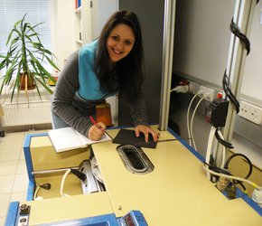
The biaxial stress-temperature measuring system “Mutti 2000” is a self-constructed facility to measure the temperature dependency of stresses in thin films. Using two parallel laser beams, the curvature resulting from the stresses of a substrate coated on one side can be measured and the stresses can be calculated. The sample is positioned in a high-vacuum chamber, enabling to investigate stress relaxation mechanisms in-situ during a thermal cycle up to 700°C. In addition to stresses and stress relaxation effects, the thermal expansion coefficient of the film can be determined from the thermal cycle.
Technical data:
- Measurement principle: cantilever beam method
- Substrate size: 20 x 7 x 0,3 mm (preferably silicon)
- Laser: Melles-Griot 3222 H-PC
- Turbomolecular-pumped vacuum chamber with radiation heaters
- Minimum pressure: 5x10⁻⁷ mbar
- Temperature: 25 - 700°C
- Heating rate: 1-20°C/min
Nanoindenter
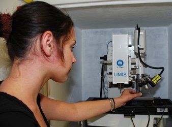
Nanoindentation is a non-destructive method that can be used to determine the hardness and elastic modulus of small volumes of material such as thin films and also bulk specimens. In nanoindentation, the depth of penetration of a diamond indenter tip or a spherical indenter is measured along with the prescribed load. The resulting load-displacement response typically shows an elastic-plastic loading followed by an elastic unloading. After careful calibration, hardness and elastic modulus of the specimen material can be calculated from the loading/unloading curves. The nanoindenter UMIS (“Indira”) is equipped with the indentation system, an optical and atomic force microscope and the data acquisition and control system. For acoustic and thermal insulation, the nanoindenter system is placed in an enclosure and positioned on a vibration damping table.
Technical data:
- Indenter: Berkovich, Vickers, spherical indenters
- Optical and atomic force microscope
- Depth range: 2 µm and 20 µm selectable
- Depth resolution: 0,003 nm (0,05nm noise floor*)
- Load range: 50 mN & 500 mN
- Minimum load: 2 µN*
- Load resolution: 0,05 µN (0,3µN noise floor*)
- Positioning stages: 0,1 µm step size
- Load frame compliance: 0,2 nm/mN
*Depends upon laboratory environment
Nanoindenter Hysitron

The mechanical properties of composite and multilayered materials can vary significantly within the micro- and nanometer scale. Thus, quantification of hardness and Young’s modulus with a high depth and lateral resolution is of major scientific and industrial relevance. In addition, modern nanoindentation devices allow to perform micro mechanical experiments on microscopic bending beams, making it possible to quantify the fracture stress and fracture toughness even for thin coatings. With the Hysitron TI 950 nanoindenter (“Herta”) it is furthermore possible to conduct hardness and Young’s modulus mappings. A fully automated indentation system, several transducers for different types of experiments and a light microscope allow sophisticated nanoindentation measurements. In addition, the surface can be scanned using the implemented tip to retrieve information on the surface morphology.
Technical data:
- Indenter: Berkovich, sphero-conical, flat-punch, cube corner
- Methodology: hardness and Young’s modulus mappings, micro-mechanical experiments, dynamic nanoindentation (CMX, CSM)
- Light microscope and scanning probe microscopy
- Load range: maximum 10 mN
- Load resolution: 30 nN
- Depth range: maximum 5 μm
- Depth resolution: 0.2 nm
- Positioning: 10 nm
Room- and high-temperature nanoindentation and micromechanics
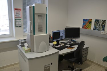
This unique high-temperature nanoindenter in a scanning electron microscope (SEM) allows local and precise measurements of the mechanical properties from room temperature up to 1000 °C. This new testing machine supports the application-oriented portfolio of the Chair of Physical Metallurgy and Metallic Materials and allows high-resolution correlation between microstructure analysis and macroscopic deformation experiments.
Technical Data:
- Manufacturer: Nanomechanics Inc. (KLA) & Tescan
- Type: In-SEM & In-SEM-HT in SEM Vega
- Testing methods: constant load rate, strain rate or displacement rate with dynamic stiffness measurement
- Load: max. 50 mN with electromagnetic load control
- Resolution: InForce50 with 3nN force resolution und 0.001 nm displacement resolution
- Testing temperature: RT – 1000°C in vacuum
Displacement-controlled cryo-nanoindenter
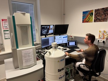
The modular design allows to use the Alemnis Standard Assembly (ASA) for in-situ and ex-situ experiments at room temperature, while the additional Low Temperature Module (LTM-CRYO) can be utilized to perform in-situ experiments at temperatures between -150 °C and 200 °C. In the ex-situ configuration, the ASA can be used as a stand-alone nanoindenter equipped with an optical microscope to navigate over the sample surface. For live observation of indentation or micromechanical experiments, the setup can be equipped to the available Tescan Vega scanning electron microscope. This in-situ configuration allows to use the LTM-CRYO module, where liquid nitrogen cooling enables controlled indentation experiments at cryogenic temperatures.
In addition to its capacity for conducting tests at cryogenic temperatures, the new indentation system distinguishes itself with its intrinsic displacement control mechanism. Unlike the load-controlled indentation systems existing at the Department, this feature enables superior control, particularly during micromechanical experiments.
Technical Data:
- Manufacturer:Alemnis AG & Tescan
- Testing methods: Intrinsically displacement controlled, constant strain rate, constant load rate via feedback loop
- Load & Resolution: max. 1.5 N & 8 µN RMS noise with SLC (standard load cell) or max. 0.5 N & 4 µN RMS noise with MLC (mini load cell)
- Displacement & Resolution: Coarse z-movement via SmarAct stage, fine z-movement via Piezostack (max. 40 µm and resolution < 1 nm)
- Testing temperature: - 150 °C – 200 °C in-situ, RT ex-situ


